As this was just flagged as a duplicate of a just closed question:
I have just uploaded a 30 page group discussion on the toner transfer method
to this dropbox file <-- FAR superior format compared to copied version below.
Have a read through there and come back and ask relevant questions if it seems to be of use.
I've posted the first 40% or so below to stop this being a link only answer.
For those interested in this method I strongly suggest you access the complete and better formated dropbox document. There is such a
vast range of material from many people in this invaluable document that it's very worth looking at.
Edit: Link updated March 2024
-------------------------------------
From: V G x.solarwind.x@gmail.com
Date: 20 March 2011 10:15
To: PICLIST piclist@mit.edu
Hi, I like the idea of direct to PCB resist printing, but don't really have
the time to modify my own printer. Does anyone know of where I can get a
pre-modified printer for this purpose?
http://www.piclist.com PIC/SX FAQ & list archive
View/change your membership options at
http://mailman.mit.edu/mailman/listinfo/piclist
From: V G x.solarwind.x@gmail.com
Date: 22 March 2011 06:38
To: PICLIST piclist@mit.edu
Hm. I guess not :(
From: Michael Watterson mike@radioway.org
Date: 22 March 2011 06:58
To: "Microcontroller discussion list - Public." piclist@mit.edu
Photo exposure is better.
Iron off laser toner next best. Discussed previously here
Any other print solution will be poor
From: V G x.solarwind.x@gmail.com
Date: 22 March 2011 08:53
To: "Microcontroller discussion list - Public." piclist@mit.edu
Sorry for not trimming, replying from phone.
You say photo exposure is best. Would you still say it's the best if
the method is using positive photo resist spray and developer? Or is
it only good when using pre-sensitized boards?
From: Michael Watterson mike@radioway.org
Date: 22 March 2011 09:10
To: "Microcontroller discussion list - Public." piclist@mit.edu
Never used the spray on. I imagine the board needs to be very clean.
polished and degreased just prior to spray.
--
From: Byron Jeff byronjeff@mail.clayton.edu
Date: 22 March 2011 11:32
To: "Microcontroller discussion list - Public." piclist@mit.edu
This is a current topic of interest for me. Basic parameters:
Single sided, one off, SMT boards for hobby prototyping. So occasional
processing (not too complicated) and ultra quick turnaround (the faster,
the better, ideally 1 hour or less) are at a premium.
Most likely targets are SOIC, 0805/0603 type parts.
KiCAD is the development target (may or may not be relevant)
What is the best method using the following priorities (in order):
Speed from printing of design to population ready.
Process repeatibility both in terms of producing a correct board with
the process and producing repeat boards using the same process. Presume
that this is the occasional hobby board, not a production setup.
Cost per board.
In short if I could print chips directly onto the PCB, that would be great.
Impossible, but great. Right now I'm looking at using a PCB hot plate type
setup for soldering. So the faster I can get setup, the faster I can get
finished.
I'm planning on testing both the Toner Transfer and the Photo resist with
precoated boards. Both seem to be about the same amount of time in terms of
speed. Overall the TT method seems to be cheaper as precoated boards seem
to run about 3x the cost. So it seems to me that the real question is
process repeatability.
Thoughts?
BAJ
Byron A. Jeff
Department Chair: IT/CS/CNET
College of Information and Mathematical Sciences
Clayton State University
http://cims.clayton.edu/bjeff
From: Bob Blick bobblick@ftml.net
Date: 22 March 2011 11:43
To: "Microcontroller discussion list - Public." piclist@mit.edu
Hi Byron,
I've tried using an XY pen plotter directly to PC board and never got
good enough etch resistance. All over the net there are recommendations
for the RED Staedtler Lumocolor pens but even they are not good enough.
I have used spray-on photoresist. It's OK except for the hairs and dust.
In other words, not good for fine pitch because you will have bad spots.
Laser toner transfer is sensitive to your ironing pressure and
temperature. I always print a border around my artwork to act as a
pressure buffer. It seems to even out the pressure near the edges. Fair
to good results if you have finesse. Prepare for lots of do-overs and
some touchup before and after etch.
Presensitized board works really well. No question, this is the way to
go if you want quality. And unlike the other methods it takes very
little talent. Your first board will be good and every one to follow.
I tend to do toner transfer because I am drawn to how immediate it
seems, and the fact that you don't really need any consumables. But then
after I have ironed on and cleaned off the same board three times before
I get a transfer good enough to etch, I rethink my choice of technology,
wishing I'd used presensitized board instead. And it's not like there
are no consumables, I use acetone to clean the board and lacquer thinner
to remove the toner.
Note to self: Since I don't make more than a dozen boards a year I
should always use the presensitized board.
Cheerful regards,
Bob
--
http://www.fastmail.fm - A no graphics, no pop-ups email service
From: Byron Jeff byronjeff@mail.clayton.edu
Date: 22 March 2011 12:41
To: "Microcontroller discussion list - Public." piclist@mit.edu
Bob,
This analysis was extremely helpful.
I started working my way through the presensitized boards the last time I
was on this roller coaster but did not complete the job. Let me run a brief
description of what I have read and see if there are any errors in my
thinking:
Print mirror of circuit onto transparancy sheet at max toner setting.
Bind sheet face down (and flat) to presensitized board. Cover with real
glass as it is transparent to UV. Do this in a low light environment.
Expose assembly to UV light. Sunlight will work but a UV light box is
better. Mine is a black light installed in a toolbox. Never got a clear
number on exposure time. Seems to be trail and error but consistent once
you get it to work.
Peel the transparancy and there should be a outline image of the circuit
on the board. Run the board through the developer (some say caustic/washing
soda is OK, others hate it. Suggestions?) until the exposed parts a
removed. Do not do it too long or risk undercutting the solid unexposed resist.
Etch the board.
Remove the rest of the photoresist. A bit unclear here. Is this a light
and develop a second time step? Or a physical process
Should be ready to shake and bake after this.
On this recommendation, I will attempt this method first. There seems to be
repeatability issues with the toner transfer method.
Thanks for the input.
BAJ
From: Oli Glaser oli.glaser@talktalk.net
Date: 22 March 2011 12:21
To: "Microcontroller discussion list - Public." piclist@mit.edu
I agree totally - I have used spray on photoresist (messy, difficult to
get even and contaminant free)
and Toner Transfer (good, but not as accurate/repeatable as photoresist)
With hot etching fluid and agitation you will get fast etching times
(~5min) and near board house resolution (we get down to around 0.2mm
trace width) after a little practice. Worth investing in a UV light box
that gives even exposure, and a decent heated etch tank. However you can
get good results with a tray in hot water and a source of UV - I used an
old sunlamp to start with, worked perfectly.
From: AK 00@case.edu
Date: 22 March 2011 12:21
To: "Microcontroller discussion list - Public." piclist@mit.edu
When using 'scuffed' shipping label backing and a laminating press,
I've found toner transfer to be very reliable and precise, even using
it for some small BGA work. Posted more details here a long time ago,
if you're interested. The good thing about using the mailing label
backing is that it peels right off, no soaking, scrubbing, or
developing needed. Just my experience.
Andrew
From: IVP joecolquitt@clear.net.nz
Date: 22 March 2011 12:30
To: "Microcontroller discussion list - Public." piclist@mit.edu
I'd agree with that. The human component is the important
variable. Repeatability and detail is there for the getting
Take these examples
PIC + quad amp + 0805 R and C. Very small text under
the 'JC 3.11' is my note for the board size. It is just about
readable (if you know what it's supposed to read. FWIW
it says, mirrored, 1.85 x 2.65 4.70 6.74 @ 600 dpi)
http://home.clear.net.nz/pages/joecolquitt/DIP+SMT.jpg
Printout (0.1" pitch pads)
http://home.clear.net.nz/pages/joecolquitt/detail.gif
Result (a little out of focus, better looking in reality)
http://home.clear.net.nz/pages/joecolquitt/detail.jpg
I read one person's account where he uses a hot-plate with a
weight to apply a known pressure for a known time. That's
something I'd like to investigate. My gauging of iron pressure
is fairly good and but I'd rather it be controlled, for a more
consistent Toner Squash Factor, which causes holes to shrink
and tracks to widen. That said, SOIC 0.05" pitch is quite
easily achievable
Joe
From: Oli Glaser oli.glaser@talktalk.net
Date: 22 March 2011 12:43
To: "Microcontroller discussion list - Public." piclist@mit.edu
Tracing paper works just as well (and is cheaper)
The UV gets through fine.
Varies with power of light (and I think resist type, so try to stick to
one) so a bit of trial and error - Good idea to print a small test
board, consisting of traces (with corners) from 1mm down to 0.1mm, a few
SMD footprints (TQFP, QFN) and some through hole pads with thin annular
rings. Expose a few of these, gradually adjusting time and note down
what works best.
I use Sodium Metasilicate, it is a lot better than Sodium Hydroxide
(Caustic Soda)
You don't have to get the timing so accurate (i.e if you leave it in a
second too long it won't strip the resist off)
Either - you can shove it under the light again then rinse in developer
(I do this way)
Or I think some folk just use an abrasive pad to clean it off, which I
do anyway afterwards to clean the copper, then run a bit of isopropyl
alcohol over it.
You can actually leave it on too I think - IIRC some resists act as a
flux, check the info/documentation on whatever board you buy. Never
tried it so not sure how it compares.
The steps you outlined look about right overall to me - this is a good
page on board making I found very helpful to begin with:
http://www.electricstuff.co.uk/pcbs.html
From: Bob Blick bobblick@ftml.net
Date: 22 March 2011 12:58
To: "Microcontroller discussion list - Public." piclist@mit.edu
I would verify if the density setting actually does anything. Every
printer is different and on mine it was turning off "economy".
Also you can use cheap 20 LB paper in a pinch if you don't have
transparencies.
I've been told inkjets work OK too, in high quality mode.
I've used glass and plexiglass and not noticed a difference. I thought
glass blocked more UV than plastic?
I have had problems peeling it off afterward. The toner sticks a little
bit.
Sunlight is nice because it is very much like a point source and you can
put the printed side out and still get focus. But if you already made a
mirror image that won't work because everything is reversed.
Timing sunlight is near impossible. I made a cumulative timer but never
got the right sensor/filter combination to match the sensitizer.
With a UV box you must get your transparency touching flat on the board
everywhere.
Timing is trial and error, but it is pretty forgiving, 2:1 once you get
in the window.
When I was teaching we made our own solution with lye. That was before
it got recognized as a component to make meth and consequently harder to
find. Now I use the recommended developer.
I am a big fan of lacquer thinner, it removes almost anything.
Cheerful regards,
Bob
--
http://www.fastmail.fm - mmm... Fastmail...
From: Bob Blick bobblick@ftml.net
Date: 22 March 2011 13:04
To: "Microcontroller discussion list - Public." piclist@mit.edu
Yes, I remember your suggestion about label backing and adopted it,
thank you.
All it takes is to ask someone who uses a UPS printer and then you have
an unlimited supply of backing paper :)
A laminating press would make a big improvement, I'm sure it would make
my boards lots more consistent.
Best regards,
Bob
--
http://www.fastmail.fm - Send your email first class
--
From: Sergey Dryga sergey@dryga.us
Date: 22 March 2011 17:31
To: piclist@mit.edu
Both glass and some plastics absorb UV, but at the thickness tipically used (~1
mm for glass) the absorbance is not too high. More important is that the glass
is "optical quality", without swirls.
I used a fluorescent lamp at 15-20 cm from the board/mask/glass stack. It was
while ago, but IIRC 75W lamp is OK. Some even reported the use of 100W
incandescent lamp. It might not work with all sensitized boards, I got mine
from Jameco, the brand is DATAK I believe.
I scrubbed with a scrubber/foam pad sold for kitchen cleaning. As last step,
200-400 grit sandpaper and water rinse. I used purified water for final rinse
since tap water often has too many minerals in it (actually I have never tested
if just tap water is OK, seems easier to just rinse in distilled water any way).
Sergey Dryga
http://beaglerobotics.com
V G x.solarwind.x@gmail.com
22 March 2011 18:45
Reply-To: "Microcontroller discussion list - Public." piclist@mit.edu
To: "Microcontroller discussion list - Public." piclist@mit.edu
On Mon, Mar 21, 2011 at 7:21 PM, AK 00@case.edu wrote:
When using 'scuffed' shipping label backing and a laminating press,
I've found toner transfer to be very reliable and precise, even using
it for some small BGA work. Posted more details here a long time ago,
if you're interested. The good thing about using the mailing label
backing is that it peels right off, no soaking, scrubbing, or
developing needed. Just my experience.
Hi. Where do you get label backing paper?
[Quoted text hidden]
AK 00@case.edu
22 March 2011 18:56
Reply-To: "Microcontroller discussion list - Public." piclist@mit.edu
To: "Microcontroller discussion list - Public." piclist@mit.edu
On Tue, Mar 22, 2011 at 2:45 AM, V G x.solarwind.x@gmail.com wrote:
On Mon, Mar 21, 2011 at 7:21 PM, AK 00@case.edu wrote:
When using 'scuffed' shipping label backing and a laminating press,
I've found toner transfer to be very reliable and precise, even using
it for some small BGA work. Posted more details here a long time ago,
if you're interested. The good thing about using the mailing label
backing is that it peels right off, no soaking, scrubbing, or
developing needed. Just my experience.
Hi. Where do you get label backing paper?
Generally free as a result of shipping other items, using this:
http://cgi.ebay.com/ws/eBayISAPI.dll?ViewItem&item=160516738494
[Quoted text hidden]
V G x.solarwind.x@gmail.com
22 March 2011 19:00
Reply-To: "Microcontroller discussion list - Public." piclist@mit.edu
To: "Microcontroller discussion list - Public." piclist@mit.edu
On Tue, Mar 22, 2011 at 2:56 AM, AK 00@case.edu wrote:
Generally free as a result of shipping other items, using this:
http://cgi.ebay.com/ws/eBayISAPI.dll?ViewItem&item=160516738494
Thanks! Are the label backings better than photo paper as recommended
everywhere?
[Quoted text hidden]
AK 00@case.edu
22 March 2011 19:43
Reply-To: "Microcontroller discussion list - Public." piclist@mit.edu
To: "Microcontroller discussion list - Public." piclist@mit.edu
On Tue, Mar 22, 2011 at 3:00 AM, V G x.solarwind.x@gmail.com wrote:
On Tue, Mar 22, 2011 at 2:56 AM, AK 00@case.edu wrote:
Generally free as a result of shipping other items, using this:
http://cgi.ebay.com/ws/eBayISAPI.dll?ViewItem&item=160516738494
Thanks! Are the label backings better than photo paper as recommended
everywhere?
I began with photo paper as described elsewhere. My experience has
been that a properly prepped backing transfers more cleanly and with
much more ease than paper. In fact, some sheets I've used multiple
times after the transfer. It's likely that you'll get finer details
with a refined optical masking process as described by others, but you
can't beat this toner transfer process for speed, cost, lack of
chemicals, and simplicity.
[Quoted text hidden]
V G x.solarwind.x@gmail.com
23 March 2011 08:52
Reply-To: "Microcontroller discussion list - Public." piclist@mit.edu
To: "Microcontroller discussion list - Public." piclist@mit.edu
On Tue, Mar 22, 2011 at 2:56 AM, AK 00@case.edu wrote:
Generally free as a result of shipping other items, using this:
http://cgi.ebay.com/ws/eBayISAPI.dll?ViewItem&item=160516738494
This is cool. I asked the guy for samples. Hopefully they work out.
[Quoted text hidden]
Ing. Marcelo Fornaso mfornaso@yahoo.com
23 March 2011 10:20
Reply-To: "Microcontroller discussion list - Public." piclist@mit.edu
To: "Microcontroller discussion list - Public." piclist@mit.edu
I'm a little afraid of using this sheets on my laser printer because their
surface looks like plastic...
Don't you think there is any risk of fusing it into the printer?
Marcelo Fornaso
From: V G x.solarwind.x@gmail.com
To: Microcontroller discussion list - Public. piclist@MIT.EDU
Sent: Tue, March 22, 2011 5:52:05 PM
Subject: Re: [EE] Direct to PCB printing (Inkjet)
[Quoted text hidden]
Robert Rolf Robert.Rolf@ualberta.ca
23 March 2011 10:30
Reply-To: "Microcontroller discussion list - Public." piclist@mit.edu
To: "Microcontroller discussion list - Public." piclist@mit.edu
There are generally two kinds of 'clear plastic' sheets out there.
The kind used for overhead transparencies, which have an absolutely
glossy surface, and which WILL melt and destroy your printer,
and those that are made of acetate, and which are a bit smoky and have a
very fine texture surface for the toner to grab on to.
If in doubt, put a soldering iron to them. The dangerous plastic will
melt nearly instantly, and stink, the 'laser' grade will curl but you'll
have to apply a fair bit of heat to melt into them.
If in doubt, don't use them.
R
Ing. Marcelo Fornaso wrote:
I'm a little afraid of using this sheets on my laser printer because their
surface looks like plastic...
Don't you think there is any risk of fusing it into the printer?
Marcelo Fornaso
[Quoted text hidden]
Bob Blick bobblick@ftml.net
23 March 2011 10:37
Reply-To: "Microcontroller discussion list - Public." piclist@mit.edu
To: "Microcontroller discussion list - Public." piclist@mit.edu
On Tue, 22 Mar 2011 15:20 -0700, "Ing. Marcelo Fornaso" wrote:
I'm a little afraid of using this sheets on my laser printer because
their
surface looks like plastic...
Don't you think there is any risk of fusing it into the printer?
With label attached it is intended to run through a printer. I haven't
ever had a problem.
It is too slippery to hold the toner until you scuff it up a little bit
with a tissue or paper towel.
I don't run it full letter size through the printer. I attach a piece
larger than the design on to a sheet of normal paper using a label at
the top of the backing paper. Center the design on the sheet so the
leading edge of the carrier paper has nothing additional on it.
Cheers,
Bob
--
http://www.fastmail.fm - A no graphics, no pop-ups email service
--
[Quoted text hidden]
Ing. Marcelo Fornaso mfornaso@yahoo.com
23 March 2011 12:05
Reply-To: "Microcontroller discussion list - Public." piclist@mit.edu
To: "Microcontroller discussion list - Public." piclist@mit.edu
Ok. I got the idea and will give it a try.
Thank you
Marcelo Fornaso
From: Bob Blick bobblick@ftml.net
To: Microcontroller discussion list - Public. piclist@mit.edu
Sent: Tue, March 22, 2011 7:37:54 PM
Subject: Re: [EE] Direct to PCB printing (Inkjet)
[Quoted text hidden]
Vic Fraenckel windswaytoo@gmail.com
23 March 2011 12:59
Reply-To: "Microcontroller discussion list - Public." piclist@mit.edu
To: "Microcontroller discussion list - Public." piclist@mit.edu
Do any of you following this thread know that there is a Yahoo Group
"Homebrew_PCB" that discusses most of the issues that you are discussing
here?
Check the group out here:
http://tech.groups.yahoo.com/group/Homebrew_PCBs/
Vic
Victor Fraenckel
KC2GUI
windswaytoo ATSIGN gmail DOT com
[Quoted text hidden]
William "Chops" Westfield westfw@mac.com
23 March 2011 13:39
Reply-To: "Microcontroller discussion list - Public." piclist@mit.edu
To: "Microcontroller discussion list - Public." piclist@mit.edu
On Mar 22, 2011, at 3:20 PM, Ing. Marcelo Fornaso wrote:
I'm a little afraid of using this sheets on my laser printer because
their
surface looks like plastic...
Sheesh. Find someplace that uses laser-printable label sheets. Or
even buy some. Use any remaining labels as ... labels or something,
leaving you with a backing sheet suitable for this sort of toner-
transfer. Any laser-printable labels will have a non-melting backing
sheet; probably silicone based.
Try the library. Our middle school library prints bar codes on sheets
of labels for their new books. This usually doesn't fill up a sheet,
and the software doesn't support exact placement of the barcodes on
partially filled sheets, so the remaining labels get stamped with the
school name/etc for tagging magazines and such. Eventually they're
all used up and the backing sheet is thrown away.
Some backing sheets are nicer than others.
I prefer the destructively processed glossy magazine paper route.
The reason that the label backing sheet works so well is that toner
doesn't stick to it. Which also can mean that it's subject to flaking
off somewhere in the process before it gets to your board...
=======
Professional PCB fabrication services get cheaper and cheaper, and
more and more convenient to amateurs. Batched hobbyist services
(batchPCB, dorkbot) have "solved" the minimum board size problem, so
that you're no longer penalized for wanting a very small board.
Direct-from-china suppliers (Itead, Seeed) are doing the cheap-
prototypes (~$20) with long lead time thing so that you're no longer
forced to use a high-priced quick-turn supplier for "prototypes." The
only remaining advantage of home fabrication is that simplicity
(single sided, 16mil design rules) will get you faster and cheaper.
But it's getting harder and hard to justify.
BillW
[Quoted text hidden]
V G x.solarwind.x@gmail.com
23 March 2011 16:45
Reply-To: "Microcontroller discussion list - Public." piclist@mit.edu
To: "Microcontroller discussion list - Public." piclist@mit.edu
On Tue, Mar 22, 2011 at 9:39 PM, William "Chops" Westfield
westfw@mac.comwrote:
[Quoted text hidden]
$20 with shipping and tax compared to a few dollars and instant turnaround
times is not hard to justify.
[Quoted text hidden]
William "Chops" Westfield westfw@mac.com
23 March 2011 17:27
Reply-To: "Microcontroller discussion list - Public." piclist@mit.edu
To: "Microcontroller discussion list - Public." piclist@mit.edu
On Mar 22, 2011, at 9:45 PM, V G wrote:
$20 with shipping and tax compared to a few dollars and instant
turnaround
times is not hard to justify.
It depends. Couple bucks for blank copper clad. Couple bucks for
etchant. Significant bucks for the high-grade ink cartridge (for
direct to PCB printing) (which may or may not dry up between PCBs (I
hate inkjets!)) or a couple bucks for special transfer paper or
transparency paper. Couple bucks for drill bits. Couple bucks for
tool to cut the PCB material. Moderate amount for an inkjet printer
to modify, or for a laminator, or for an iron, or for a contact
exposure frame. Couple buck for other chemicals, sandpaper, etc.
I dunno. I've spent a couple $K for an LPKF (mill) to get that
"instant turnaround." But it's not really that "instant", and I'm
increasingly uncertain that it was a worthwhile purchase.
BillW
[Quoted text hidden]
V G x.solarwind.x@gmail.com
23 March 2011 20:17
Reply-To: "Microcontroller discussion list - Public." piclist@mit.edu
To: "Microcontroller discussion list - Public." piclist@mit.edu
On Wed, Mar 23, 2011 at 1:27 AM, William "Chops" Westfield
westfw@mac.comwrote:
It depends. Couple bucks for blank copper clad.
Agreed.
Couple bucks for etchant.
That's a one time thing. A bottle will last a LONG time. If you use the
HCL/H2O2 method, you can make it last forever and it's VERY cheap.
Significant bucks for the high-grade ink cartridge (for
direct to PCB printing) (which may or may not dry up between PCBs (I
hate inkjets!))
Or, just a laser printer (that most people have anyway) on label backing
paper that you can get for free.
or a couple bucks for special transfer paper or
transparency paper.
It'll last you a lifetime.
Couple bucks for drill bits.
Tungsten carbide bits will last you pretty much forever and they're pretty
cheap.
Couple bucks for tool to cut the PCB material.
Again, it'll last you forever.
Moderate amount for an inkjet printer
to modify, or for a laminator, or for an iron, or for a contact
exposure frame. Couple buck for other chemicals, sandpaper, etc.
Sandpaper costs pennies, most people already have a laser printer, most
people have a clothes iron.
I dunno. I've spent a couple $K for an LPKF (mill) to get that
"instant turnaround." But it's not really that "instant", and I'm
increasingly uncertain that it was a worthwhile purchase.
So what you only really need is the copper board. Everything is already
lying around somewhere or will last "forever" or costs pennies.
[Quoted text hidden]
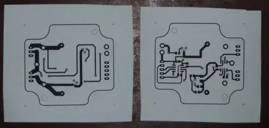 The bottom (left) and top (right) of a simple double-sided board (the top one is printed out mirrored so they overlay when its turned over). Normally I would print onto the blue Press-n-Peel film, just using paper here for illustration.
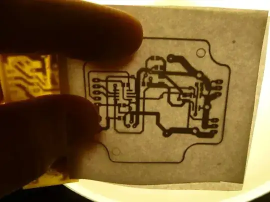 With one side taped to the scrap PCB (left side) and the printed sides facing each other, hold them up to the light and align the other one so that all the holes and the board outline line up.
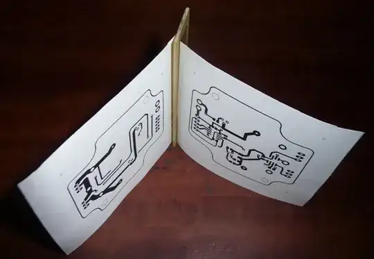 Here they are both stuck to the PCB scrap. You can now put the clean blank PCB between the two (probably best to tape it to both sides to avoid any movement) and run it through the laminator (or iron it) to transfer the toner onto the PCB.
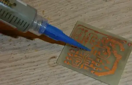