0

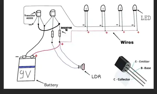
Could you please help me by checking whether this circuit diagram is correct for connection digram.

Kindly ignore resistor R2 330 R (as it is not included in the connection diagram)

Actually I am a beginner in the electronics.diagram 1diagram 2

Muser996
  • 1
  • 2
  • Q1 CE is reversed in layout,, make layout like schematic in future for logical appearance, until you can make fewer DRC errors (design check) and add REF DES Q1 Q2 to assy dwg. etc – Tony Stewart EE75 Dec 22 '19 at 16:42
  • You do need a 330 Ohm (or so) resistor in series with each LED, like R2, to limit the LELD current to a safe value. – Peter Bennett Dec 22 '19 at 16:49
  • @PeterBennett that omission is covered in question but triggered a power saving idea. 4 Reds=8V (approx) so put in series with 1V/20mA = 50 Ohms min. for R2 or two 100R in // – Tony Stewart EE75 Dec 22 '19 at 16:54
  • 1
    No, it’s not correct and you should work harder at seeing the differences. With EE, the devil is in the detail. That’s every detail, even the smallest. – Andy aka Dec 22 '19 at 17:00
  • @Tony Stewart "Q1 CE is reversed in layout", Do you mean the labels on transistor in the top image to the lower right-hand side?? – Muser996 Dec 22 '19 at 17:09
  • The schematic shows the emitters of both transistors connected to the negative terminal of the battery, but your wiring sketch shows the emitter of the left transistor and collector of the right transistor connected to battery negative. – Peter Bennett Dec 22 '19 at 17:20
  • by Layout , I meant physical layout (top) vs logical layout (schematic) We call it Murphy's Law. If anything can be backwards , it will be. – Tony Stewart EE75 Dec 22 '19 at 17:27
  • Thank you all for the clarification. – Muser996 Dec 22 '19 at 17:30
  • I've already done something like it, with hysteresis, here. Just FYI in case you care. If you want to see an entirely different approach, also with hysteresis but also with some more design discussion included, you could also go here. There are lots of ways to go. But I think all of them should include some hysteresis. – jonk Dec 22 '19 at 19:16

2 Answers2

1

Ok,

First, I'm not exactly sure what your asking, but it sounds like the question is if the top diagram(connection) is an accurate rendition of the bottom diagram(schematic). Do I have that correct?

Second, even though I hate the stuff, I would recommend that at a minimum that you take a look at Fritzing.

Now for an answer.

No, the two barely have any correlation.
1. Why are you trying to run it at 9V instead of the requested 6V? That is only 4 batteries(AAA, AA, C or D) in series. 2. As constructed on the top diagram, you'll burn ALL of those LED's, at once. 3. Eeekkk..

For a better circuit that uses a 9V battery, check out this page, plus it only has ONE transistor and a good explanation.

GB - AE7OO
  • 1,073
  • 7
  • 19
0

The transistor Q1 is biased with the help of LDR and a known resistance. When the LDR has low resistance (day time), there is enough current into the base which enables beta*Ib current to flow into the collector. This current causes high drop in voltage across the resistor, leaving very less voltage for the second transistor's base.

Since the voltage at second base is not enough to allow current through, no current flows through the base and collector(ideally). So your LED can't get enough current to light up.

When LDR has high resistance, there is no current through 1st base and collector. So your 2nd base gets enough voltage to allow enough current to pass through it and causes higher current to pass through the collector. So your LED can light up.

G-aura-V
  • 1,069
  • 1
  • 8
  • 22
  • Thank you so much to explain how this system works, but I was asking if the second diagram could be used for the top diagram or there I cannot as there is a big difference between them – Muser996 Dec 22 '19 at 18:41