I'm really confused with the representation of PMOS device shown in the figure. Since conventional current direction in PMOS is from source to drain, shouldn't the current source be pointing upwards(from node Y to VDD)?
I'm really confused with the representation of PMOS device shown in the figure. Since conventional current direction in PMOS is from source to drain, shouldn't the current source be pointing upwards(from node Y to VDD)?
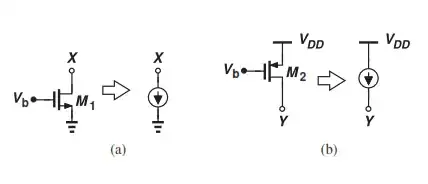
Simplest way to remember current direction is by the little arrow indicator on the transistor, for NMOS it is pointing out of the drain thus current flows from source to drain. And for PMOS the arrow is into the source, so flows from source to drain. It is important to remember that the source is indicated by the arrow location. So in the case drawn, NMOS source is on the bottom and PMOS source is on the top.
Mosfets can be confusing at times. The main difference between the pmos and the nmos is whether you need to apply a positive or negative Vgs to form a channel. The current will always flow from the higher potential to the lower potential (so from vdd to gnd) and never the other way around. In fact when you look at the device physics, a mosfet is pretty symmetrical. Using names like drain and source are just conventions. The arrow is therefore pointing in the right direction.